About Atrix
Lorem ipsum dolor amet consectetur adipisicing sed do eiusmod tempor incididunt labore magna aliqua enim minim veniam nostrud exercitation aboris nis aliquip exeo.
Find Us Our Location
- 629 12th St, Modesto, CA 95354 United States
- atrixmain@gmail.com
- +1 (230)-456-155-23
Blog Standard

Revolutionizing Semiconductor Failure Analysis with Nenovision’s LiteScope AFM-in-SEM
As semiconductor devices continue to shrink in size and grow in complexity, the demand for precise and efficient Semiconductor Failure Analysis has never been greater. Identifying defects at the nanoscale level is critical to ensuring the performance, reliability, and yield of modern electronics, from NAND flash memory to advanced transistors. Nenovision’s LiteScope, an innovative Atomic Force Microscope (AFM) integrated into a Scanning Electron Microscope (SEM), offers a transformative solution. By combining Hybrid imaging for semiconductor analysis with a seamless in-situ workflow, LiteScope empowers researchers and engineers to address failure analysis challenges with unparalleled accuracy and speed.
The Power of Hybrid Imaging for Semiconductor Analysis
The LiteScope combines the strengths of Atomic Force Microscopy and Scanning Electron Microscopy within a FIB/SEM environment, offering a seamless workflow for Semiconductor inspection tools. This hybrid approach delivers high-resolution conductivity mapping and dopant profiling without compromising sample integrity. By merging sample preparation and analysis, it eliminates the risks of surface oxidation and contamination, ensuring accurate results. The system is compatible with SEM systems from leading manufacturers such as Thermo Fisher Scientific, TESCAN, ZEISS, Hitachi, and JEOL, making it a versatile addition to existing failure analysis workflows.
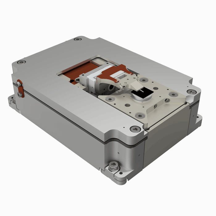
NenoVision LiteScope
Key Benefits of LiteScope
- Site-Specific Analysis: The LiteScope enables precise conductivity mapping and dopant concentration analysis of specific vias, interconnections, and transistors, using SEM for accurate localization.
- In-Vacuum Workflow: Fully integrated into the FIB/SEM environment, the system streamlines processes, preventing contamination and enhancing efficiency.
- Probe Protection and Accessibility: A docking station preserves the AFM tip during Focused Ion Beam (FIB) milling, while a Sample Rotation Module ensures optimal positioning for complex geometries.
- Time and Cost Efficiency: By reducing measurement time per sample, LiteScope accelerates research and development, making it a cost-effective solution for Semiconductor Failure Analysis.
Applications in Semiconductor Failure Analysis
The LiteScope is designed for critical applications such as NAND failure analysis, SRAM and logic circuits, transistors (FinFET, CMOS), and thin films. For instance, in NAND failure analysis, the system identifies specific vias in a NAND structure, performs sequential delayering using Plasma-Focused Ion Beam (PFIB), and conducts electrical analysis via Conductive AFM (C-AFM) and I/V Spectroscopy. This in-situ approach allows real-time monitoring of the delayering process, ensuring precise targeting and revealing electrical failures at various depths.
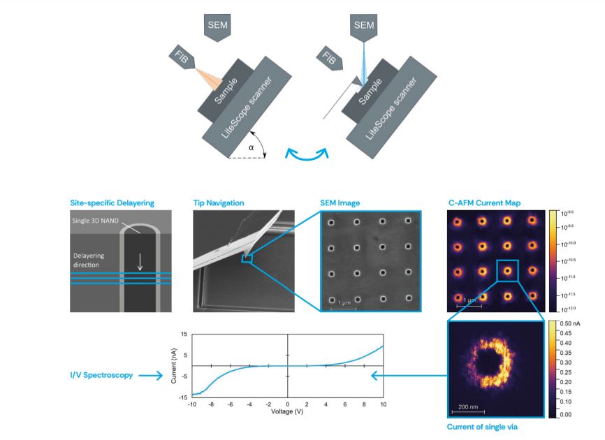
Fig 1 In-situ electrical failure analysis of NAND structures
Scanning Spreading Resistance Microscopy for Dopant Analysis
A standout feature of the LiteScope is its ability to perform Scanning Spreading Resistance Microscopy (SSRM) for dopant concentration analysis. By correlating SEM imaging with local electrical properties, SSRM provides nanoscale precision in mapping variations in doping levels, which are critical for device performance and reliability. For SiC MOSFET transistors, this technique enables detailed characterization of doped layers and junctions, analyzing their shape, size, and depth to ensure optimal conductivity and minimal losses.
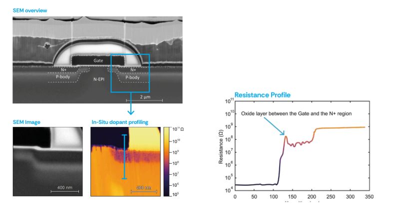
Fig 2 Site-Specific Dopant Concentration Analysis of MOSFET Transistor
Workflow for Comprehensive Failure Analysis
The Failure Analysis with AFM-in-SEM LiteScope begins with site-specific sample preparation using FIB to expose defect areas. The AFM tip is then navigated to the region of interest for high-resolution electrical characterization, such as C-AFM or SSRM. Results are correlated with SEM imaging, and calibration is performed using reference resistance measurements on samples with known dopant concentration levels. This calibration ensures accurate dopant profiling, providing a comprehensive understanding of failure mechanisms.
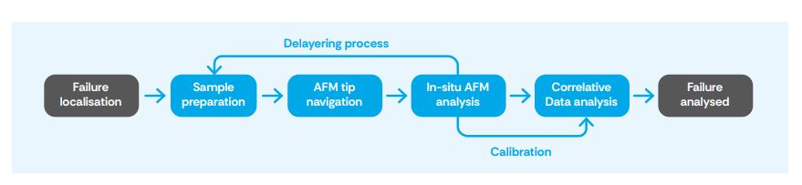
Fig 3 Failure analysis workflow with AFM-in-FIB/SEM
Enhancing Device Performance and Reliability
By combining AFM-in-SEM techniques like C-AFM, SSRM, and complementary SEM methods (e.g., EBIC, EBAC), the LiteScope enhances defect detection and accelerates failure diagnostics. This integrated approach significantly reduces time-to-result, improves manufacturing yield, and supports the development of more reliable semiconductor devices.
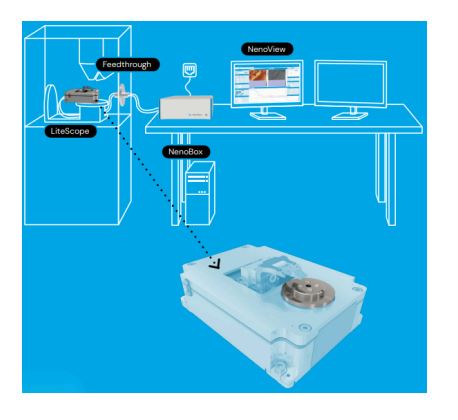
Fig4 NenoVision LiteScope Setup
Conclusion
In an era where semiconductor innovation drives technological progress, Nenovision’s LiteScope stands out as a game-changer in Nanoscale metrology for chips. By integrating AFM-in-SEM capabilities, it offers a robust solution for Semiconductor Failure Analysis, delivering precise conductivity mapping, dopant profiling, and enhanced device performance and reliability. With its ability to streamline workflows, reduce costs, and provide actionable insights, LiteScope empowers manufacturers to overcome the challenges of modern semiconductor design.
Inkarp Instruments is a top distributor and reliable service partner for NenoVision products in India. Driven by a commitment to innovation and excellence, Inkarp offers advanced scientific instruments along with professional support, enabling researchers across the country to push the boundaries of scientific discovery.
References:NenoVision